
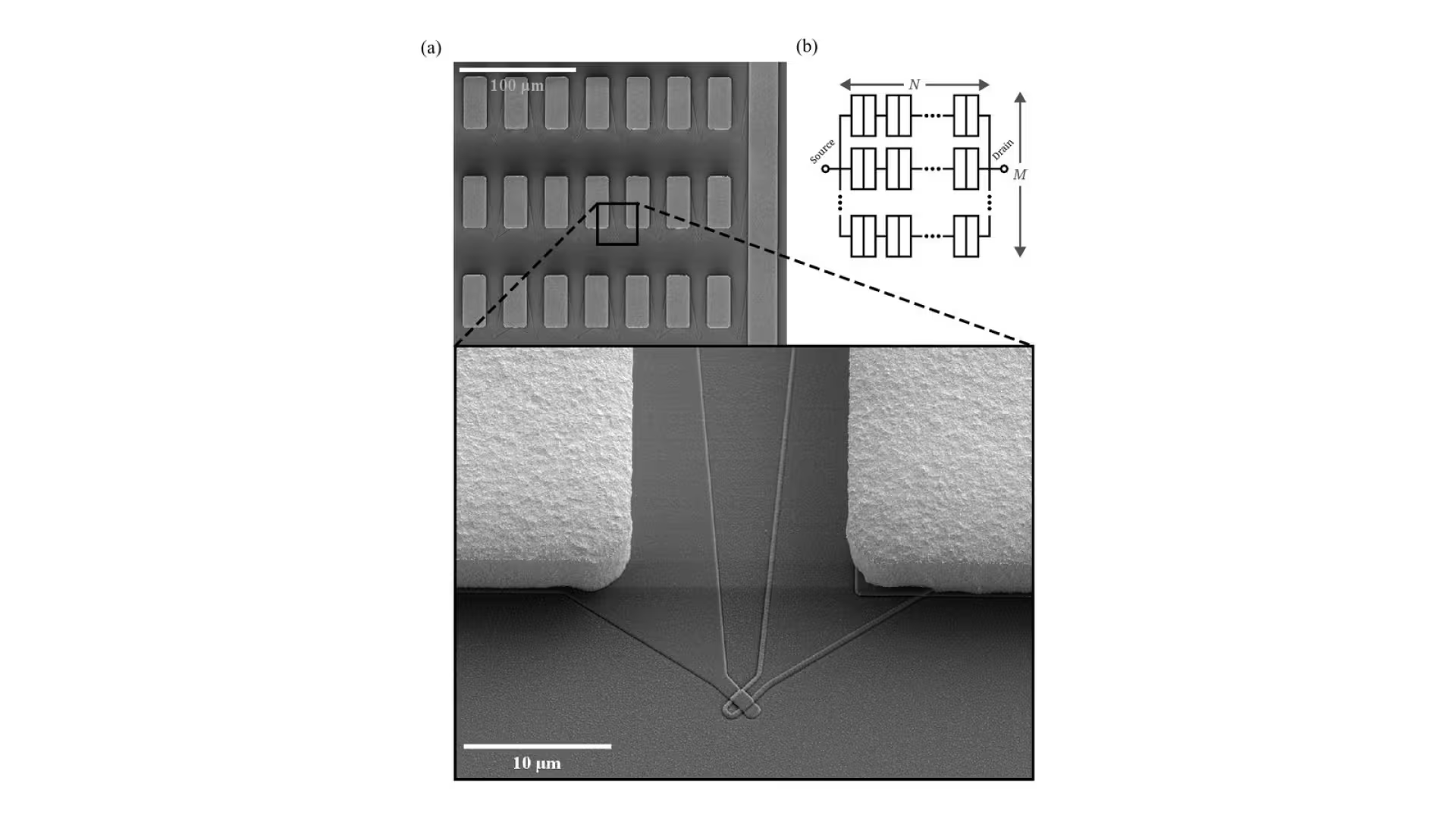
Characterising cryogenic devices is slow: a traditional cryostat holds only a few samples, and one measurement cycle can take days. Researchers at VTT Technical Research Centre of Finland, working with Bluefors, have demonstrated wafer-scale characterisation below one kelvin using a 300 mm cryogenic wafer prober.
They measured Coulomb blockade thermometers made with VTT's recently developed TiW/Al-AlOx/TiW normal-metal tunnel junction technology and, using primary thermometry, found on-chip electron temperatures below 700 mK across a full 150 mm wafer. Wafer-level testing below 1 K could enable high-throughput screening of quantum devices and aluminium-based superconducting circuits. The team included Lassi Lehtisyrjä, Renan Loreto, Juho Luomahaara and Mika Prunnila.
The preprint has not yet been peer reviewed.
Figure: Lehtisyrjä et al., arXiv:2609.12596 (2026)